


3D графика. Что это такое
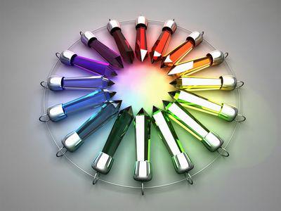
3D графика или трёхмерная графика – это один из разделов компьютерной графики, комплекс приемов и инструментов, которые позволяют создать объемные объекты при помощи форма и цвета. От двухмерных изображений она отличается тем, что подразумевает построение геометрической проекции трехмерной модели сцены (виртуального пространства) на плоскость, делается это при помощи специализированных программ. Полученная модель может соответствовать объектам реального мира (например, здание, человек, автомобиль, астероид) или быть целиком абстрактной (проекция четырехмерного фрактала).
Сегодня 3D графика прочно вошла во многие сферы нашей жизни – это:
- строительство (визуализация объемных архитектурных изображений зданий, объектов, интерьера, экстерьера);
- производство (объектное моделирование);
- телевидение (моделированные фото в глянцевых журналах, видеоролики, спецэффекты в кино),
- игровая индустрия (3D-анимация и виртуальные миры, разработка компьютерных игр);
- полиграфия (создание полиграфической продукции),
- реклама (электронные презентации и каталоги, рекламные щиты и пр.) и т.д.
3D-графика - один из наиболее эффективных инструментов в рекламе, позволяющий расширить влияние на потенциального клиента и повысить качество преподносимой рекламы как реальном, так и в виртуальном мире.
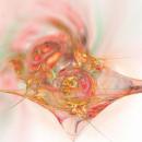
О фракталах и их алгоритмах
Понятия фрактал и фрактальная геометрия, появившиеся в конце 70-х, с середины 80-х прочно вошли в обиход математиков и программистов
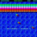
Amegas
Но как бы то ни было, после этого игровой рынок вновь пережил наплыв клонов Арканоида, ведь многие игроки второй половины 80-х и слыхом не слыхивали о старинной игре Breakout
Создание сложных объектов в 3ds max 7
Многие объекты, которые окружают нас в повседневной жизни, имеют несимметричную поверхность, воспроизвести которую в трехмерной графике довольно сложно
Выбор бюджетного 3D-телевизора. Рейтинг 5 лучших моделей
Думается, эта статья может быть полезна как тем, кто задумался о новогоднем подарке, так и тем, кто ищет второй телевизор в дом и хотел бы, чтобы он был с поддержкой 3D, дабы иметь возможность посмотреть свежие 3D-фильмы


